You just pulled a brand-new ESP32 out of its packaging, soldered it onto your board, uploaded your code, and... nothing. The serial monitor is silent. The module draws current but refuses to boot. You order another one, and this time it works — so you blame the first one on "a defective unit" and move on with your life.
Here is the uncomfortable truth: you probably killed it yourself. Not with a soldering iron mishap or a reversed power supply. You killed it with your fingertip, and you never even felt it happen.
Welcome to the world of Electrostatic Discharge — the invisible, silent, and absurdly common destroyer of electronic components.
What Is Electrostatic Discharge?
Electrostatic Discharge (ESD) is the sudden flow of electricity between two objects at different electrical potentials. In simpler terms, it is a tiny spark — sometimes visible, often not — that occurs when accumulated static charge finds a path to ground.
You have experienced ESD countless times. That sharp zap when you touch a doorknob after walking across a room? That is ESD. The small shock when you slide out of a car seat and touch the metal door frame? Also ESD.
These events feel like minor annoyances to you. To a semiconductor, they are catastrophic.
The Voltage Problem: Numbers That Should Terrify You
Here is what makes ESD so dangerous: the voltages involved are enormous relative to what electronic components can survive.
| Activity | Typical Voltage Generated |
|---|---|
| Walking across a carpet | 4,000 - 35,000V |
| Walking across a vinyl floor | 250 - 12,000V |
| Sliding off a plastic chair | 1,500 - 18,000V |
| Picking up a plastic bag from a bench | 1,200 - 20,000V |
| Removing a component from a plastic tube | 500 - 2,000V |
| Handling bubble wrap or thermocol | 1,200 - 26,000V |
Now compare those numbers to what your components can actually withstand:
| Component | ESD Damage Threshold |
|---|---|
| MOSFET (gate oxide) | 100 - 200V |
| CMOS IC (e.g., 74HC series) | 250 - 2,000V |
| ESP32 / ESP8266 | 500 - 1,000V (GPIO pins) |
| Op-amps (JFET input) | 150 - 500V |
| Schottky diodes | 300 - 1,000V |
| Precision ADCs | 500 - 1,500V |
| OLED / LCD display drivers | 100 - 500V |
The critical detail: you cannot feel an ESD event below approximately 3,000V. That means you can discharge 2,000V into a MOSFET — twenty times its survival threshold — and feel absolutely nothing. No spark. No zap. No indication whatsoever that you just destroyed a component.
How ESD Actually Damages Components
ESD does not simply "fry" a component in the way most people imagine. The damage mechanisms are specific, and understanding them helps you appreciate why certain components are more vulnerable than others.
Gate Oxide Breakdown (MOSFETs and CMOS)
MOSFETs work by applying a voltage to an extremely thin gate oxide layer — often just a few nanometers thick. This layer is an insulator, and it is astonishingly fragile. An ESD pulse punches through this oxide layer like a needle through tissue paper, creating a permanent conductive path. The transistor is now shorted, and no amount of wishful thinking will fix it.
This is why MOSFETs are among the most ESD-sensitive components in existence.
Junction Damage (Diodes and ICs)
In bipolar transistors, diodes, and many ICs, ESD current flows through semiconductor junctions. The energy is concentrated in a microscopically small area, causing localized melting of the silicon. This creates short circuits or changes the electrical characteristics of the junction permanently.
Metallization Damage
Inside an IC, the metal traces connecting different parts of the circuit are incredibly thin. A high-current ESD pulse can literally melt these traces, creating open circuits within the chip. From the outside, the IC looks perfectly fine. Inside, it is broken beyond repair.
The Worst Kind: Latent Damage
This is the scenario that should keep you up at night. Not all ESD events cause immediate failure. Some weaken a component without killing it outright. The gate oxide develops a micro-crack. A junction is partially damaged. The component passes all your tests, works in your prototype, and then fails three weeks or three months later in the field.
Latent ESD damage is estimated to account for a significant portion of "random" field failures in electronic products. The component worked on your bench, passed QC, shipped to your customer, and then died. You blame the component manufacturer. The real culprit was the static charge on your fingertip during assembly.
Vulnerability Ranking: What Is Most at Risk?
Most Vulnerable (Handle With Extreme Care)
- MOSFETs — Both discrete and those inside ICs. The thin gate oxide is the weakest link.
- CMOS ICs — This includes nearly all modern digital logic: microcontrollers, memory chips, FPGAs.
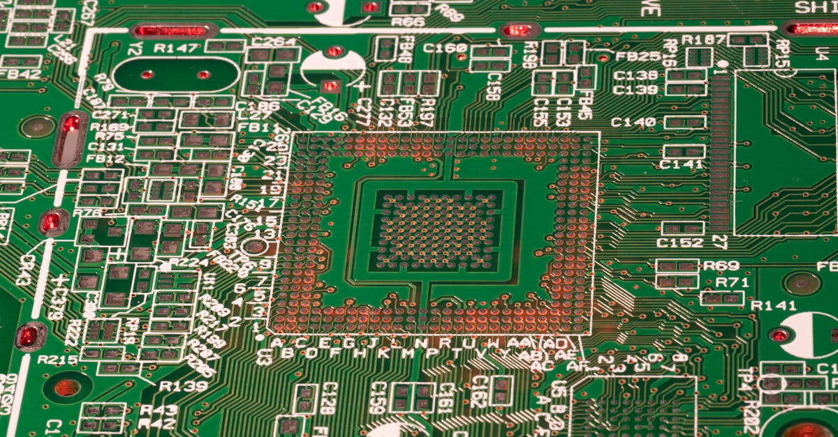
- ESP32 and ESP8266 modules — Built on CMOS process technology. The GPIO pins are directly connected to the die with minimal internal protection on many pins.
- MEMS sensors — Accelerometers, gyroscopes, and pressure sensors with microscopic mechanical structures.
- Precision analog ICs — Op-amps with FET inputs, ADCs, DACs. Their performance depends on precise junction characteristics that ESD disrupts.
- LED driver ICs — Constant-current drivers and PWM controllers with sensitive gate structures.
- Bare display panels — OLED and TFT-LCD panels with thin-film transistors on glass.
Moderately Vulnerable
- Bipolar transistors — More robust than MOSFETs but still susceptible to junction damage.
- Standard diodes — Generally tougher, but Schottky diodes are more sensitive.
- Voltage regulators — Internal MOSFET pass elements can be damaged.
Least Vulnerable
- Resistors — Both through-hole and SMD resistors are essentially immune to ESD at workbench levels.
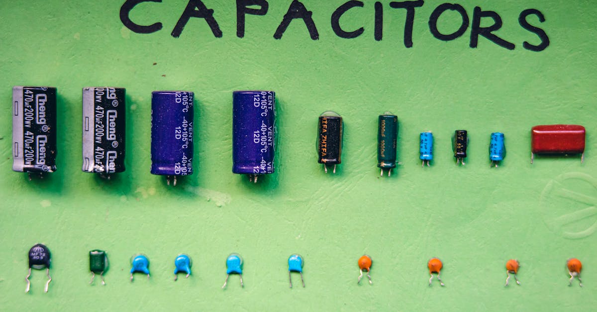
- Ceramic and electrolytic capacitors — Passive components with no semiconductor junctions.
- Through-hole LEDs — Simple P-N junctions with relatively robust construction.
- Inductors and transformers — Wire wound around a core. ESD is not a concern.
- Connectors and mechanical switches — Metal and plastic. ESD-proof by nature.
Prevention at the Workbench
Anti-Static Wrist Strap
This is the single most effective ESD prevention tool, and it costs less than a cup of chai.
How it works: A conductive band around your wrist connects through a coiled cable to an earth ground point. This keeps your body at the same electrical potential as your workbench and components, preventing charge buildup.
How to use it properly:
- The strap must make skin contact — wear it snug against your wrist, not over your sleeve.
- The cable must connect to a true earth ground. The ground pin of a three-pin wall socket works. A metal water pipe that goes into the ground works. The metal case of a grounded appliance works.
- The cable contains a 1M-ohm resistor — this is a safety feature that limits current if you accidentally touch mains voltage. Never bypass this resistor. Never connect yourself directly to ground without it.
- Test the strap periodically. Stretch the band, check the snap connection, and verify continuity with a multimeter.
Cost: Rs. 50 - 200
ESD-Safe Work Mat
A grounded conductive or dissipative mat placed on your workbench provides a safe surface for components and PCBs.
Key points:
- The mat must be grounded — an ungrounded mat is just a green rubber sheet that does nothing useful.
- Connect the mat's ground snap to the same earth point as your wrist strap.
- The mat drains charge slowly (dissipative, not conductive) to avoid creating its own ESD events.
Cost: Rs. 300 - 800 for a standard bench-size mat
Anti-Static Bags and Packaging
Not all anti-static bags are created equal:
| Bag Type | Appearance | Protection Level | Use Case |
|---|---|---|---|
| Pink poly bag | Translucent pink | Low — prevents triboelectric charging only | Storing non-critical parts, resistors, connectors |
| Static shielding bag | Metallic/silver with grid pattern | High — creates a Faraday cage effect | ICs, MOSFETs, microcontrollers, sensitive modules |
| Black conductive bag | Opaque black | Medium-high — conductive exterior | Populated PCBs, field-replaceable modules |
Important: A static shielding bag only protects the component inside it. Placing a component on top of a shielding bag provides zero protection — the metallic exterior is conductive, and you could actually discharge through the bag into the component.
Humidity: Your Invisible Ally (or Enemy)
Static charge accumulates far more readily in dry air. At 60-70% relative humidity, the thin layer of moisture on surfaces provides a natural discharge path that bleeds off static before it accumulates to dangerous levels. Below 30% humidity, static charge builds up aggressively.
Indian climate considerations:
- November through February: North India experiences dry winters with humidity often dropping below 30%. This is peak ESD season. Delhi, Jaipur, Lucknow, and the entire Indo-Gangetic plain become static charge factories during these months.
- Air-conditioned rooms year-round: AC units pull moisture out of the air. A comfortable 24 degrees C room with the AC running can easily drop below 35% humidity. If you work in an AC environment in Bangalore or Hyderabad, you are not immune to ESD just because you live in a "humid" city.
- Synthetic clothing: Polyester shirts and nylon jackets are triboelectric nightmares. Cotton generates far less static. If you are doing sensitive electronics work, wear cotton.
Practical tip: A simple room humidifier near your workbench can make a measurable difference. You are not trying to turn your room into a tropical greenhouse — just keeping humidity above 40% dramatically reduces ESD risk.
The Quick Ground Touch
Before handling any sensitive component, touch a grounded metal object. This is not a substitute for a wrist strap, but it is vastly better than nothing. Touch the metal chassis of a grounded instrument, the metal body of your oscilloscope, or a grounded metal shelf bracket.
This discharges your body at that instant — but you start accumulating charge again the moment you shift in your chair or adjust your clothing. That is why a wrist strap, which provides continuous grounding, is superior.
Handling Best Practices
- Hold PCBs by the edges. Your fingers should never touch component leads, IC pins, or exposed traces.
- Never touch IC pins directly. If you need to insert an IC into a socket, hold it by the plastic body.
- Keep components in their anti-static packaging until the exact moment you need them. Do not open a bag of MOSFETs and leave them sitting on your desk "for convenience."
- Do not slide components across surfaces. Sliding generates triboelectric charge. Lift and place.
- Pass components to another person by placing them on the ESD mat, not hand-to-hand.
- Avoid thermocol (expanded polystyrene) and bubble wrap near your workspace. These materials generate extreme static charges. Use them for shipping, not for workbench storage.
ESD Protection in Circuit Design
Even with perfect handling practices, your finished product will encounter ESD in the real world. Users will touch connectors, cables will be plugged and unplugged, and static-charged objects will come near your circuit. Designing in ESD protection is not optional for any product that leaves your bench.
TVS Diodes on I/O Pins
Transient Voltage Suppressor (TVS) diodes are the frontline defense. Place them on any pin that connects to the outside world: USB data lines, UART, SPI, I2C, GPIO connected to buttons or sensors, and power input.
A TVS diode sits dormant during normal operation. When an ESD event occurs, it clamps the voltage to a safe level in nanoseconds, diverting the energy to ground.
Recommended approach: Use a TVS array IC like the TPD4E05U06 (Texas Instruments), which protects four lines in a single tiny package. It is rated for IEC 61000-4-2 Level 4 (contact discharge of +-8kV) and costs very little per channel.
Series Resistors on GPIO
A simple 100-ohm to 1K-ohm resistor in series with a GPIO pin limits the peak current during an ESD event. Combined with the internal ESD protection diodes present on most microcontrollers, this can be enough for many applications.
This is especially useful for ESP32 GPIO pins connected to external connectors, buttons, or sensor cables that users might touch.
Proper Grounding
Your circuit's ground plane is the return path for ESD energy. A solid, unbroken ground plane on your PCB gives ESD current a low-impedance path to follow, reducing the voltage that develops across sensitive components.
Never route sensitive signal traces near board edges where ESD is most likely to enter. Keep your ground plane continuous under connector footprints.
Dedicated ESD Protection ICs
For USB, HDMI, Ethernet, and other standardized interfaces, dedicated ESD protection ICs are available that are designed specifically for the signal characteristics of that interface. They add minimal capacitance and do not degrade signal integrity.
Testing for ESD Damage
How do you know if a component has been ESD-damaged? Unfortunately, there is no simple "ESD damage detector." But here are signs:
- Component is completely dead — no response, draws excessive current, or draws no current at all.
- Intermittent behavior — works sometimes, fails randomly, resets unexpectedly. This is the hallmark of latent damage.
- Degraded analog performance — an ADC that used to be accurate now has excessive noise or offset. An op-amp with increased input bias current.
- Increased leakage current — measurable with a sensitive multimeter on MOSFET gate-source or IC supply pins.
- GPIO pins that are "stuck" — an ESP32 where certain GPIO pins no longer respond to code while others work fine. Individual pin damage is a classic ESD signature.
If you suspect ESD damage, the honest answer is: replace the component. A partially damaged component is worse than a dead one because it introduces unpredictable behavior into your system.
Building an ESD-Safe Workspace on a Budget
You do not need a professional electronics factory setup. Here is what a basic ESD-safe hobby workspace costs in India:
| Item | Approximate Cost | Priority |
|---|---|---|
| Anti-static wrist strap (with cable and resistor) | Rs. 80 - 200 | Essential |
| ESD-safe mat (60cm x 40cm, with ground cord) | Rs. 300 - 600 | Essential |
| Grounding point adapter (banana-to-croc clip for wall socket ground pin) | Rs. 50 - 100 | Essential |
| Static shielding bags (pack of 50, various sizes) | Rs. 150 - 300 | Important |
| Anti-static component storage boxes | Rs. 100 - 300 | Important |
| Conductive foam sheet (for IC storage) | Rs. 50 - 150 | Nice to have |
| Room humidifier (ultrasonic, small) | Rs. 500 - 1,000 | Seasonal |
Total for a solid basic setup: Rs. 580 - 1,200. That is less than the cost of two ESP32 modules. If you have ever had a "defective" component arrive dead on arrival, this investment pays for itself immediately.
Setting Up the Ground Point
The most critical part of the setup is establishing a reliable earth ground connection:
- Identify a three-pin wall socket. Verify the earth pin is actually connected — in many Indian installations, it is not. Use a socket tester or multimeter to check continuity between the earth pin and a known ground (metal water pipe going into the earth).
- Use a grounding cord with a ring terminal or croc clip to connect to the earth pin.
- Connect both your wrist strap and ESD mat to this same ground point.
Common Myths — Debunked
"I have been building electronics for years and never had ESD damage."
You almost certainly have. You attributed it to "defective components," "bad solder joints," or "weird firmware bugs." Studies in professional electronics manufacturing suggest that 25-30% of component failures are ESD-related. The percentage in hobby settings, where ESD precautions are rarely taken, is likely higher.
"Touching the metal case of my computer is enough."
Only if the computer is plugged in and the case is truly grounded. And even then, it only discharges you at that instant. The moment you shift in your seat or reach for a component across the desk, you have built up charge again. A single touch is a point-in-time discharge, not continuous protection.
"ESD only matters in dry climates."
ESD risk is lower in humid environments, but it does not disappear. An AC room in Chennai during July can have lower humidity than a winter day in Shimla. And synthetic clothing generates static regardless of ambient humidity.
"Components have built-in ESD protection, so I do not need to worry."
Many modern ICs do include internal ESD protection structures — typically rated for 1,000 to 2,000V HBM (Human Body Model). But these structures protect against brief, incidental contact, not against repeated exposure or higher-voltage events. Walking across a carpet can generate 20,000V. Internal protection is a last line of defense, not a substitute for proper handling.
"Anti-static bags protect components when you place them on the bag."
False and dangerous. The outer surface of a metallic shielding bag is conductive. Placing a sensitive component on top of the bag is like placing it on a sheet of metal — it provides no protection and can actually facilitate discharge. Components must be inside the bag with the opening sealed or folded over.
Storage and Organization
- ICs and MOSFETs: Store in conductive foam (the black foam that ICs ship in). Each pin is shorted to every other pin through the foam, preventing differential voltage buildup. Never use regular white Styrofoam — it generates massive static charge.
- Loose components: Use anti-static component boxes with compartments. Label clearly.
- PCBs: Store in static shielding bags or anti-static bins. Do not stack bare PCBs on top of each other.
- Reels and tubes: SMD component reels and IC tubes are generally anti-static by design. Keep them sealed until use.
ESD Standards Reference
If you are designing products for commercial sale or want to understand the formal specifications:
| Standard | Description |
|---|---|
| IEC 61000-4-2 | International standard for ESD immunity testing of electronic equipment. Defines test levels from +-2kV to +-8kV contact discharge. |
| HBM (Human Body Model) | ANSI/ESDA/JEDEC JS-001. Simulates a person touching a component. Models the human body as a 100pF capacitor discharged through a 1.5K-ohm resistor. |
| CDM (Charged Device Model) | ANSI/ESDA/JEDEC JS-002. Simulates the component itself being charged and then touching ground — the more realistic scenario in automated assembly. |
| MM (Machine Model) | Simulates discharge from manufacturing equipment. Less commonly referenced today but still relevant. |
For hobby and small-scale production, aiming for IEC 61000-4-2 Level 2 (+-4kV contact discharge) on all external interfaces is a reasonable and achievable target.
Final Thought
ESD is not dramatic. There is no smoke, no visible damage, no satisfying pop to tell you something went wrong. It is the most mundane and invisible failure mode in electronics — and precisely because of that, it is the most commonly ignored.
A Rs. 100 wrist strap and five minutes of discipline can save you from hours of debugging phantom failures, wasted components, and the slow erosion of trust in your own work. When a circuit behaves erratically and you cannot find the bug, the first question should always be: did I handle these components properly?
Protect your components. They cannot protect themselves.